- 您现在的位置:买卖IC网 > Sheet目录479 > MRF89XA-I/MQ (Microchip Technology)TXRX ISM SUB-GHZ ULP 32QFN
�� �
�
�MRF89XA�
�4.8� General� PCB� Layout� Design�
�The� following� guidelines� can� be� used� to� assist� in� high-�
�frequency� PCB� layout� design.�
�The� printed� circuit� board� is� usually� comprised� of� two� or�
�four� basic� FR4� layers.�
�The� two-layer� printed� circuit� board� has� mixed� signal/�
�power/RF� and� common� ground� routed� in� both� the� lay-�
�ers� (see� Figure� 4-8� ).�
�The� four-layer� printed� circuit� board� (see� Figure� 4-9� )� is�
�comprised� of� the� following� layers:�
�?� Signal� layout�
�?� Thorough� decoupling� on� each� power� pin� is�
�beneficial� for� reducing� in-band� transceiver� noise,�
�particularly� when� this� noise� degrades� performance.�
�Usually,� low� value� caps� (27-47� pF)� combined� with�
�large� value� caps� (100� nF)� will� cover� a� large�
�spectrum� of� frequency.�
�?� Passive� component� (inductors)� should� be� in� the�
�high-frequency� category� and� the� Self-Resonant�
�Frequency� (SRF)� should� be� at� least� two� times�
�higher� than� the� operating� frequency.�
�?� The� additional� trace� length� affects� the� crystal�
�oscillator� by� adding� parasitic� capacitance� to� the�
�overall� load� of� the� crystal.� To� minimize� this,� place�
�?�
�?�
�RF� ground�
�Power� line� routing�
�the� crystal� as� close� as� possible� to� the� RF� device.�
�?� Setting� short� and� direct� connections� between� the�
�?� Common� ground�
�The� following� guidelines� explain� the� requirements� of�
�the� previously� mentioned� layers:�
�?� It� is� important� to� keep� the� original� PCB� thickness,�
�because� any� change� will� affect� antenna� perfor-�
�mance� (see� total� thickness� of� dielectric)� or�
�microstrip� lines’� characteristic� impedance.�
�?� For� good� transmit� and� receive� performance,� the�
�trace� lengths� at� the� RF� pins� must� be� kept� as� short�
�as� possible.� Using� small,� surface� mount� compo-�
�nents� (in� 0402/0603� package)� yields� good� perfor-�
�mance� and� keeps� the� RF� circuit� small.� RF�
�connections� should� be� short� and� direct.�
�?� Except� for� the� antenna� layout,� avoid� sharp� corners�
�because� they� can� act� as� an� antenna.� Round� corners�
�will� eliminate� possible� future� EMI� problems.�
�?� Digital� lines� are� prone� to� be� very� noisy� when� han-�
�dling� periodic� waveforms� and� fast� clock/switching�
�rates.� Avoid� RF� signal� layout� close� to� any� of� the�
�digital� lines.�
�?� A� VIA� filled� ground� patch� underneath� the� IC�
�transceiver� is� mandatory.�
�?� The� power� supply� must� be� distributed� to� each� pin� in�
�a� star� topology,� and� low-ESR� capacitors� must� be�
�placed� at� each� pin� for� proper� decoupling� noise.�
�components� on� board� minimizes� the� effects� of�
�“frequency� pulling”� that� might� be� introduced� by� stray�
�capacitance.� It� even� allows� the� internal� load� capaci-�
�tance� of� the� chip� to� be� more� effective� in� properly�
�loading� the� crystal� oscillator� circuit.�
�?� Long� run� tracks� of� clock� signal� may� radiate� and�
�cause� interference.� This� can� degrade� receiver� per-�
�formance� and� add� harmonics� or� unwanted�
�modulation� to� the� transmitter.�
�?� Keep� clock� connections� as� short� as� possible� and�
�surround� the� clock� trace� with� an� adjacent� ground�
�plane� pour.� Pouring� helps� in� reducing� any� radiation�
�or� crosstalk� due� to� long� run� traces� of� the� clock�
�signal.�
�?� Low� value� decoupling� capacitors,� typically� 0.01-0.1�
�μF,� should� be� placed� for� V� DD� of� the� chip� and� for� bias�
�points� of� the� RF� circuit.�
�?� High� value� decoupling� capacitors,� typically� 2.2-10�
�μF,� should� be� placed� at� the� point� where� power� is�
�applied� to� the� PCB.�
�?� Power� supply� bypassing� is� necessary.� Poor� bypass-�
�ing� contributes� to� conducted� interference,� which� can�
�cause� noise� and� spurious� signals� to� couple� into� the�
�RF� sections,� significantly� reducing� the� performance.�
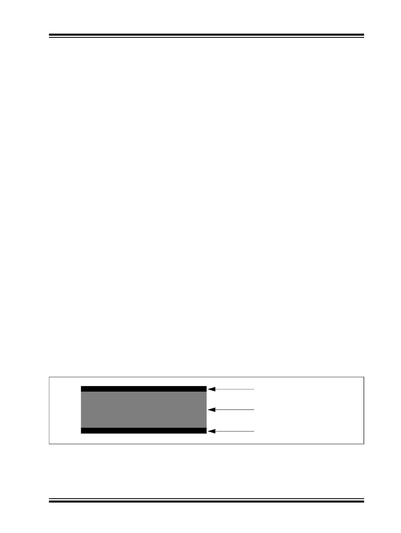
�FIGURE� 4-8:�
�TWO� BASIC� COPPER� FR4� LAYERS�
�Signal/Power/RF� and�
�Common� Ground�
�Dielectric� Constant� =� 4.5�
�Signal/Power/RF� and�
�Common� Ground�
�?� 2010–2011� Microchip� Technology� Inc.�
�Preliminary�
�DS70622C-page� 101�
�发布紧急采购,3分钟左右您将得到回复。
相关PDF资料
MRF89XAM9A-I/RM
IC TXRX MOD 915MHZ ULP SUB-GHZ
MRX-001-433DR-B
MODULE RECEIVER 433MHZ 18DIP
MRX-002-433DR-B
MODULE RECEIVER 433MHZ 18DIP
MRX-002SL-433DR-B
MODULE RCVR 433MHZ SAW LN 24DIP
MRX-005-915DR-B
MODULE RECEIVER 915MHZ 18DIP
MRX-005SL-915DR-B
MODULE RCVR 915MHZ SAW LN 24DIP
MRX-007-433DR-B
MODULE RECEIVER 433MHZ 18DIP
MRX-008-433DR-B
MODULE RECEIVER 433MHZ 18DIP
相关代理商/技术参数
MRF89XAM8A-I
制造商:MICROCHIP 制造商全称:Microchip Technology 功能描述:Ultra Low-Power, Integrated ISM Band Sub-GHz Transceiver
MRF89XAM8A-I/RM
功能描述:射频模块 868MHz Sub-GHz transceiver module
RoHS:否 制造商:Linx Technologies 产品:Transceiver Modules 频带:902 MHz to 928 MHz 输出功率:- 15.5 dBm to + 12.5 dBm 接口类型:UART 工作电源电压:- 0.3 VDC to + 5.5 VDC 传输供电电流:38.1 mA 接收供电电流:22.7 mA 天线连接器类型:U.FL 最大工作温度:+ 85 C 尺寸:1.15 mm x 0.63 mm x 0.131 mm
MRF89XAM8A-I/RM
制造商:Microchip Technology Inc 功能描述:, Leaded Process Compatible:Yes, Peak Re
MRF89XAM9A_12
制造商:MICROCHIP 制造商全称:Microchip Technology 功能描述:915 MHz Ultra Low-Power Sub-GHz Transceiver Module
MRF89XAM9A-I/RM
功能描述:射频模块 915MHz Sub-GHz Transceiver Mod RoHS:否 制造商:Linx Technologies 产品:Transceiver Modules 频带:902 MHz to 928 MHz 输出功率:- 15.5 dBm to + 12.5 dBm 接口类型:UART 工作电源电压:- 0.3 VDC to + 5.5 VDC 传输供电电流:38.1 mA 接收供电电流:22.7 mA 天线连接器类型:U.FL 最大工作温度:+ 85 C 尺寸:1.15 mm x 0.63 mm x 0.131 mm
MRF89XAM9AT-I/RM
制造商:Microchip Technology Inc 功能描述:915 MHz Ultra Low-Power Sub-GHz Transceiver Module
MRF89XAT-I/MQ
功能描述:射频收发器 868/915/950 MHz Sub-GHz transceiver RoHS:否 制造商:Atmel 频率范围:2322 MHz to 2527 MHz 最大数据速率:2000 Kbps 调制格式:OQPSK 输出功率:4 dBm 类型: 工作电源电压:1.8 V to 3.6 V 最大工作温度:+ 85 C 接口类型:SPI 封装 / 箱体:QFN-32 封装:Tray
MRF8HP21080HR3
功能描述:射频MOSFET电源晶体管 HV8 2.1GHZ 160W NI780H-4 RoHS:否 制造商:Freescale Semiconductor 配置:Single 晶体管极性: 频率:1800 MHz to 2000 MHz 增益:27 dB 输出功率:100 W 汲极/源极击穿电压: 漏极连续电流: 闸/源击穿电压: 最大工作温度: 封装 / 箱体:NI-780-4 封装:Tray